
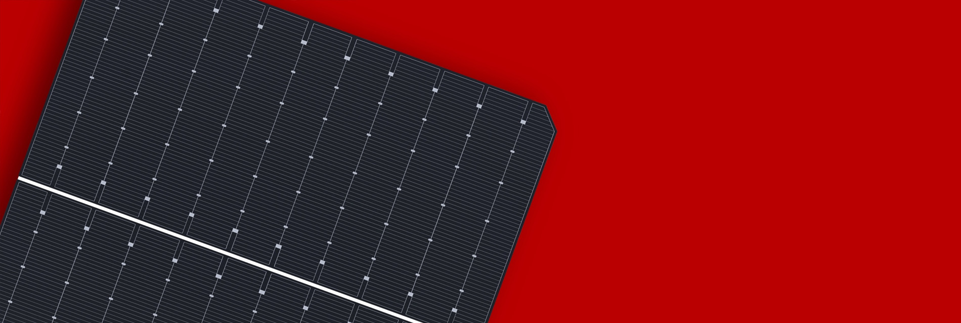
ALTAIRON™ PERC SE SOLAR CELL | P-Type
Advanced Efficiency with P-Type Technology
Altairon™ PERC SE (Passivated Emitter and Rear Cell – Selective Emitter) solar cells represent an advanced photovoltaic technology that combines two cutting-edge approaches to enhance performance and efficiency. By integrating the PERC (Passivated Emitter and Rear Cell) technology with the Shingled Emitter design, PERC SE cells achieve superior efficiency and reliability. PERC technology reduces electron recombination losses through a passivated emitter and rear layer, while the Shingled Emitter design segments the cell into overlapping strips.
Altairon™ PERC technology enhances efficiency by incorporating a passivated emitter and rear layer, which significantly reduces electron recombination losses. The passivated emitter minimizes surface recombination, ensuring fewer energy losses at contact points, while the rear layer further improves light absorption and energy conversion.
Meanwhile, the Selective Emitter design optimizes performance by cutting the solar cell into overlapping strips that are seamlessly interconnected. This design reduces shading and resistive losses, allowing for better current flow and improved overall efficiency.
P-type PERC solar cells use boron-doped silicon wafers, forming a P-N junction with a negatively charged N-type layer on top. When sunlight hits the cell, it generates electron-hole pairs, which are separated by the electric field at the junction, producing electrical current. P-type cells are cost-effective, widely used, and highly reliable, making them a key foundation for modern photovoltaic technology. With their passivated contact structures and selective emitter architecture, PERC SE solar cells deliver enhanced power output, efficiency, and long-term stability, making them an excellent choice for high-performance solar energy systems.
TECHNOLOGY FEATURES AND FUNCTIONS
Altairon™ PERC SE solar cells incorporate several advanced features designed to enhance efficiency and performance. These features collectively enable PERC SE solar cells to achieve higher efficiency, superior performance in diverse conditions, and greater durability compared to traditional solar cells. Key features include:
- Passivated Emitter Layer: Reduces electron recombination losses, enhancing overall efficiency.
- Silicon Wafer: Acts as the core material for converting sunlight into electrical energy.
- Anti-Reflective Coating (ARC): Reduces light reflection, increasing light absorption.
- Front Contact Grid: Minimizes shading and resistive losses while collecting electrical current.
- Passivated Rear Layer: Further reduces recombination losses on the rear side.
- Rear Reflector: Reflects light back into the silicon wafer to improve absorption.
- Rear Contact Grid: Enhances current collection from the back surface.
- Selective Emitter Design: Segments the cell into overlapping strips that are interconnected, reducing shading and resistive losses.
TECHNOLOGY BENEFITS
Altairon™ PERC SE solar cells offer enhanced efficiency, increased power output, improved performance, and greater durability, due to their advanced design. The passivated emitter and rear cell design reduces recombination losses and boosts efficiency with light-reflective layers, while the selective emitter design minimizes shading and resistive losses, maximizing energy production. Their performance remains strong in both high temperatures and low-light conditions, and their durable design ensures mechanical stability and longevity. Additionally, these cells provide a modern aesthetic and reduce overall costs through fewer panels and lower installation and maintenance expenses, making them a reliable and cost-effective choice for various solar energy applications.
Enhanced Efficiency

Increased Power Output

Improved Performance

Better Durability

Increased Reliability

Beautiful Aesthetics

Cost Effective

Investment Confidence